- 您现在的位置:买卖IC网 > Sheet目录1971 > UPD78F1168AGF-GAS-AX (Renesas Electronics America)MCU 16BIT 78K0R/KX3 100-LQFP
CHAPTER 4 PORT FUNCTIONS
User’s Manual U17894EJ9V0UD
105
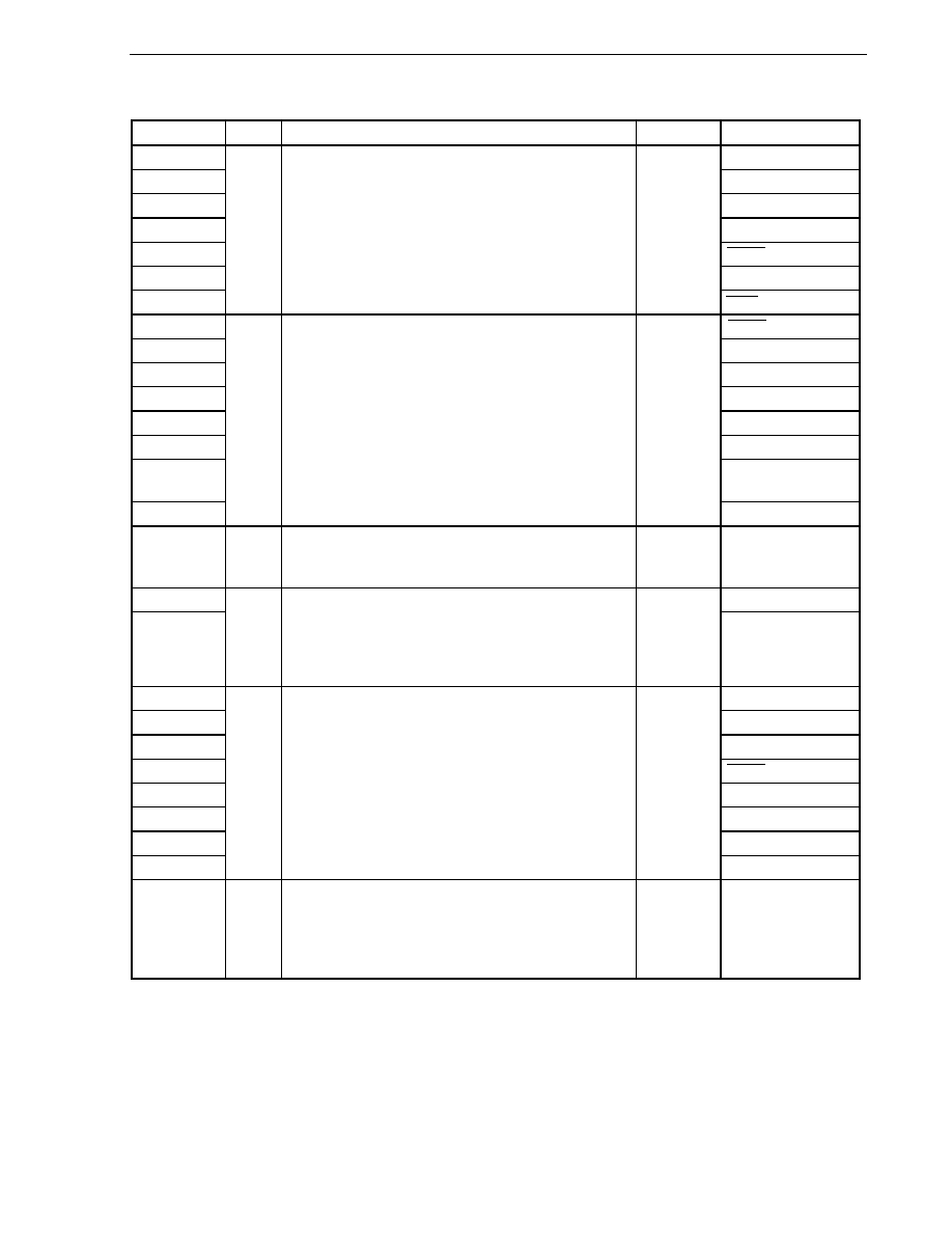
Table 4-2. Port Functions (1/2)
Function Name
I/O
Function
After Reset
Alternate Function
P00
TI00
P01
TO00
P02
SO10/TxD1
P03
SI10/RxD1/SDA10
P04
SCK10/SCL10
P05
CLKOUT
P06
I/O
Port 0.
7-bit I/O port.
Input of P03 and P04 can be set to TTL input buffer.
Output of P02 to P04 can be set to N-ch open-drain output
(VDD tolerance).
Input/output can be specified in 1-bit units.
Use of an on-chip pull-up resistor can be specified by a
software setting.
Input port
WAIT
P10
SCK00/EX24
P11
SI00/RxD0/EX25
P12
SO00/TxD0/EX26
P13
TxD3/EX27
P14
RxD3/EX28
P15
RTCDIV/RTCCL/EX29
P16
TI01/TO01/INTP5/
EX30
P17
I/O
Port 1.
8-bit I/O port.
Input/output can be specified in 1-bit units.
Use of an on-chip pull-up resistor can be specified by a
software setting.
Input port
TI02/TO02/EX31
P20 to P27
I/O
Port 2.
8-bit I/O port.
Input/output can be specified in 1-bit units.
Digital input
port
ANI0 to ANI7
P30
RTC1HZ/INTP3
P31
I/O
Port 3.
2-bit I/O port.
Input/output can be specified in 1-bit units.
Use of an on-chip pull-up resistor can be specified by a
software setting.
Input port
TI03/TO03/INTP4
P40
Note
TOOL0
P41
TOOL1
P42
TI04/TO04
P43
SCK01
P44
SI01
P45
SO01
P46
INTP1/TI05/TO05
P47
I/O
Port 4.
8-bit I/O port.
Input of P43 and P44 can be set to TTL input buffer.
Output of P43 and P45 can be set to N-ch open-drain output
(VDD tolerance).
Input/output can be specified in 1-bit units.
Use of an on-chip pull-up resistor can be specified by a
software setting.
Input port
INTP2
P50 to P57
I/O
Port 5.
8-bit I/O port.
Input/output can be specified in 1-bit units.
Use of an on-chip pull-up resistor can be specified by a
software setting.
Input port
EX8 to EX15
Note If on-chip debugging is enabled by using an option byte, be sure to pull up the P40/TOOL0 pin externally
(see Caution in 2.2.5 P40 to P47 (port 4)).
发布紧急采购,3分钟左右您将得到回复。
相关PDF资料
UPD78F1178AGF-GAT-AX
MCU 16BIT 78K0R/KX3 128-LQFP
UPD78F1188AGJ-GAE-AX
MCU 16BIT 78K0R/KX3 144-LQFP
UPD78F1235GK-GAJ-AX
MCU 16BIT 78K0R/LX3 64-LQFP
UPD78F4225YGC-8BT-A
MCU 16BIT 128K FLASH
UPD78F9202MA-CAC-A
MCU 8BIT 4KB FLASH 128B RAM
UPD78F9212CS-CAB-A
MCU 8BIT 4KB FLASH 16PIN
UPD78F9222CS-CAC-A
MCU 8BIT 4KB FLASH 20PIN
UPD78F9234CS-CAA-A
MCU 8BIT 8KB FLASH 30PIN
相关代理商/技术参数
UPD78F1168GC-UEU-AX
制造商:Renesas Electronics Corporation 功能描述:
UPD78F1168GF-GAS-AX
制造商:Renesas Electronics Corporation 功能描述:
UPD78F1174AGF-GAT-AX
功能描述:MCU 16BIT 78K0R/KX3 128-LQFP RoHS:是 类别:集成电路 (IC) >> 嵌入式 - 微控制器, 系列:78K0R/Kx3 标准包装:250 系列:80C 核心处理器:8051 芯体尺寸:8-位 速度:16MHz 连通性:EBI/EMI,I²C,UART/USART 外围设备:POR,PWM,WDT 输入/输出数:40 程序存储器容量:- 程序存储器类型:ROMless EEPROM 大小:- RAM 容量:256 x 8 电压 - 电源 (Vcc/Vdd):4.5 V ~ 5.5 V 数据转换器:A/D 8x10b 振荡器型:内部 工作温度:-40°C ~ 85°C 封装/外壳:68-LCC(J 形引线) 包装:带卷 (TR)
UPD78F1174GF-GAT-AX
制造商:Renesas Electronics Corporation 功能描述:
UPD78F1175AGF-GAT-AX
功能描述:MCU 16BIT 78K0R/KX3 128-LQFP RoHS:是 类别:集成电路 (IC) >> 嵌入式 - 微控制器, 系列:78K0R/Kx3 标准包装:250 系列:80C 核心处理器:8051 芯体尺寸:8-位 速度:16MHz 连通性:EBI/EMI,I²C,UART/USART 外围设备:POR,PWM,WDT 输入/输出数:40 程序存储器容量:- 程序存储器类型:ROMless EEPROM 大小:- RAM 容量:256 x 8 电压 - 电源 (Vcc/Vdd):4.5 V ~ 5.5 V 数据转换器:A/D 8x10b 振荡器型:内部 工作温度:-40°C ~ 85°C 封装/外壳:68-LCC(J 形引线) 包装:带卷 (TR)
UPD78F1176AGF-GAT-AX
功能描述:MCU 16BIT 78K0R/KX3 128-LQFP RoHS:是 类别:集成电路 (IC) >> 嵌入式 - 微控制器, 系列:78K0R/Kx3 标准包装:250 系列:80C 核心处理器:8051 芯体尺寸:8-位 速度:16MHz 连通性:EBI/EMI,I²C,UART/USART 外围设备:POR,PWM,WDT 输入/输出数:40 程序存储器容量:- 程序存储器类型:ROMless EEPROM 大小:- RAM 容量:256 x 8 电压 - 电源 (Vcc/Vdd):4.5 V ~ 5.5 V 数据转换器:A/D 8x10b 振荡器型:内部 工作温度:-40°C ~ 85°C 封装/外壳:68-LCC(J 形引线) 包装:带卷 (TR)
UPD78F1177AGF-GAT-AX
功能描述:MCU 16BIT 78K0R/KX3 128-LQFP RoHS:是 类别:集成电路 (IC) >> 嵌入式 - 微控制器, 系列:78K0R/Kx3 标准包装:250 系列:80C 核心处理器:8051 芯体尺寸:8-位 速度:16MHz 连通性:EBI/EMI,I²C,UART/USART 外围设备:POR,PWM,WDT 输入/输出数:40 程序存储器容量:- 程序存储器类型:ROMless EEPROM 大小:- RAM 容量:256 x 8 电压 - 电源 (Vcc/Vdd):4.5 V ~ 5.5 V 数据转换器:A/D 8x10b 振荡器型:内部 工作温度:-40°C ~ 85°C 封装/外壳:68-LCC(J 形引线) 包装:带卷 (TR)
UPD78F1177AGF-GAT-E2-AX
制造商:Renesas Electronics Corporation 功能描述: